
 Product
 Brand
Brand Articles
 Tools
Tools
Latches, Flip-Flops, Registers and Buffers
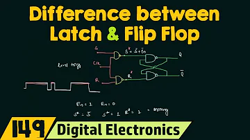
Difference between Latch and Flip Flop
| Topics covered in this article: |
| Ⅰ. What is Latch? |
| Ⅱ. What is Flip Flop? |
| Ⅲ. What is Register? |
| Ⅳ. What is Buffer? |
| Ⅴ. What is the difference between a latch and a flip-flop? |
Ⅰ. What is Latch?
Latch is a type of latch that is sensitive to the pulse level and changes state in response to the clock pulse level.
The latch is a storage unit that is activated when a certain level is reached. The data storage action is determined by the level of the input clock (or enable) signal. The output will only vary with the data entered if the latch is enabled.
(To put it another way, it has two inputs: an effective signal EN and an input data signal DATA IN, as well as an output Q whose role is to pass the value of DATA IN to Q when EN is valid, i.e. the locking process.)
The latch is not the same as the flip-flop. The signal at the output terminal fluctuates with the input signal when it is not latching the data, just like the signal flows through a buffer; once the latch signal functions as a latch, the data is locked and the input signal does not. When not locked, latches are sometimes known as transparent latches since the output is transparent to the input.
Application: The data is valid at a later time than the clock signal. This signifies that the clock signal comes first, followed by the data signal. In some arithmetic circuits, latches are employed as data scratchpads.
Disadvantage: Timing analysis is difficult.
There are two reasons why latches aren't used: 1. Glitches are common with latches. 2. With ASIC (application-specific integrated circuit) design, latches are easier than ff (flip-flops), but in FPGA resources, most devices lack a latch, necessitating the use of a logic gate and ff to create a latch, wasting resources. (Using CPLDs (Complex Programmable Logic Devices) with FPGA s is one of the most common approaches to developing ASICs) (Field Programmable Logic Arrays)
Advantages: compact size. Because the latch is faster than the FF, it is ideal for address latching, but all latch signal sources must be of high quality. The latch is widely used in CPU architecture, and it is due to its utilization that the processor's speed is boosted. External IO component logic is much slower. Because latches require fewer gates to perform the same function as flip-flops, they are more commonly utilized in asics.
Ⅱ. What is Flip Flop?
Flip-flop: (Flip-Flop, abbreviated as FF), also known as bistable gate, or bistable flip-flop, is a digital logic circuit that has two states. Flip-flops maintain their state until an input pulse, also known as triggers, is received. The trigger output changes state according to the rules when an input pulse is received and then stays in that state until another trigger is received.
For digital integrated circuits (ICs) that use memory chips and microprocessors, flip-flop circuits are coupled to produce logic gates. They can be used to store a single byte of information. This information might be anything from the status of the sequencer to the value of a counter to the ASCII letters stored in the computer's memory.
T (toggle), S-R (set/reset), J-K (also known as Jack Kilby ), and D (delay) are some of the different types of flip-flops circuits (delay). Zero, one, or two input signals, as well as clock and output signals, are common in flip-flops. An explicit input signal that resets the current output is included in some flip-flops. The first electronic trigger was devised in 1919 by W.H.Eccles and F.W.Jordan.
Flip-flop—a device that is sensitive to pulse edges and whose state changes only when a clock pulse rises or falls.
A T flip-flop (also known as a toggle flip-flop or a trigger flip-flop) has two inputs and outputs. If T and Q are different when the clock frequency changes from 0 to 1, the output value will be 1. T is the input terminal.
When it is 1, the output terminal's state Q is reversed; when the input terminal T is 0, the output terminal's state Q remains unchanged. To make a T flip-flop, connect the J and K input points of the JK flip-flop together.
Application: The clock is accurate later than the data. This means that the data signal is established first, followed by the clock signal. At the rising edge of CP, into the register.
Ⅲ. What is Register?
Register: It is widely used in many digital systems and computers to temporarily store data and operation results involved in the operation. In truth, a register is a standard sequential logic circuit, but it simply has a storage circuit. Because a latch or flip-flop can store a 1-bit binary integer, the register's storage circuit is made up of latches or flip-flops. N latches or flip-flops can form an N-bit register. The project's registers are often constructed based on the number of bytes in the computer, therefore there are 8-bit registers, 16-bit registers, and so on.
A register can be built with any flip-flop that has the purpose of setting 1 and 0, whether it is a synchronous RS structure flip-flop, a master-slave structure flip-flop, or an edge-triggered structure flip-flop. It features a common input/output enable control terminal and clock and is typically made up of D flip-flops. In most cases, the enable control terminal serves as the register circuit's selection signal, while the clock control terminal serves as the data input control signal.
The data involved in the operation, as well as the operation outcomes, are temporarily stored in some modest storage spaces. It's found in a variety of digital systems and computers. In truth, a register is a standard sequential logic circuit, but it simply has a storage circuit. The register's storage circuit is made up of latches or flip-flops. N latches or flip-flops can form an N-bit register since each latch or flip-flop can store a 1-bit binary value. The project's registers are often constructed based on the number of bytes in the computer, therefore there are 8-bit registers, 16-bit registers, and so on.
A register can be built with any flip-flop that has the purpose of setting 1 and 0, whether it is a synchronous RS structure flip-flop, a master-slave structure flip-flop, or an edge-triggered structure flip-flop. It features a common input/output enable control terminal and clock and is typically made up of D flip-flops. In most cases, the enable control terminal serves as the register circuit's selection signal, while the clock control terminal serves as the data input control signal.
Application of registers:
1. It can convert data from parallel to serial and serial to parallel; 2. It can be used as a display data latch: many devices require the counter's count value to be displayed, which is counted using the 8421BCD code and displayed on a seven-segment display. The human eye cannot distinguish the quickly changing display characters if the counting speed is high. A popular way for controlling the data display time is to add a latch between the counter and the decoder.
2. Functions as a buffer;
3. Counter composition: Shift registers are made up of shift-type counters like a ring or twisted ring counters.
Register a shift register is a register having a shifting function.
The only purpose of a register is to store data or code. It is sometimes essential to shift each bit of data in the register by one bit to the high or low order under the operation of the shift control signal in order to process data. According to the digital movement direction, which can regulate the bidirectional (reversible) shift register, the shift register is classified as left shift or right shift; according to the data input terminal and output mode, it is classified as serial or parallel. In addition to D-edge flip-flops, JK flip-flops can be utilized to create shift registers.
Ⅳ. What is Buffer?
Buffer register: Register a shift register is a register having a shifting function.
The only purpose of a register is to store data or code. It is sometimes essential to shift each bit of data in the register by one bit to the high or low order under the operation of the shift control signal in order to process data. According to the digital movement direction, which can regulate the bidirectional (reversible) shift register, the shift register is classified as left shift or right shift; according to the data input terminal and output mode, it is classified as serial or parallel. In addition to D-edge flip-flops, JK flip-flops can be utilized to create shift registers. The former's job is to temporarily store data sent by the peripheral so that the processor may retrieve it; the latter's job is to temporarily store data sent by the processor to the peripheral. The numerical control buffer allows the high-speed CPU and slow-speed peripherals to coordinate and buffer data transmission synchronization.
Buffer:
A buffer is a storage region that is utilized to transport data between devices that have different beginning speeds or priorities. The buffer reduces mutual waiting between processes, ensuring that when data is read from the slow device, the fast device's operating process is not disrupted.
The term "buffer" refers to a computer field. A circuit with a latch structure or a circuit without a latch structure can construct the buffer in terms of the specific implementation. In general, when the working speeds of sending and receiving data are the same, a circuit without a latch structure can be used to implement the buffer; when the working speeds of sending and receiving data are not the same, a buffer with a latch structure is employed. to achieve a circuit (otherwise, there will be data loss).
Buffers have many uses in digital systems:
(1) If the device's load capacity is limited, a buffer with a driver can be added; (2) If the logic levels between the front and rear stages differ, a level converter can be used to match them.
(3) Use an inverting buffer when the logic polarity is different or a unisexual variable needs to be transformed to a complementary variable; (4) Use a Schmitt circuit to convert a slowly changing signal into a signal with a steep edge.
(5) When data transmission and processing differ due to temperature and time differences between devices, add the first-level buffer to compensate, etc.
Ⅴ. What is the difference between a latch and a flip-flop?
Latches and flip-flops are binary storage devices with memory functions that are used to construct various sequential logic circuits. The latch is connected to all of its input signals, and the latch changes when the input signal changes; the flip-flop is controlled by the clock, and the current input is sampled and the output is generated only when the clock is activated. Because both the latch and the flip-flop are sequential logic devices, the output is tied to both the current input and the output from the preceding time.
1. The latch is asynchronously regulated and level-triggered. The latch is identical to a channel when the enable signal is valid, and the latch preserves the output state when the enable signal is invalid. DFF is controlled synchronously and is triggered by the clock edge.
2. Because the latch is sensitive to the input level and is strongly influenced by the wiring delay, it's difficult to verify that the output is free of burrs; DFF is difficult to generate burrs.
3. When the gate circuit is utilized to construct the latch and DFF, the latch utilizes fewer gate resources than the DFF, demonstrating the latch's superiority over the DFF. As a result, the integration level of employing latch in ASIC is higher than that of DFF, while the converse is true in FPGA. where there is no standard latch unit but a DFF unit, and one LATCH requires many LEs to actualize. The latch is level-triggered, which is equal to having an enable terminal, and it is equivalent to a wire that changes with the output after activation (when the level is enabled). in a state of disability
The next step is to maintain the original signal, which can be seen as different from a flip-flop. In many circumstances, the latch cannot replace flip-flop.
4. Static timing analysis is complicated by the latch.
5. The latch is currently only found in very high-end circuits, such as Intel's P4 and other CPUs. The FPGA has a latch unit, and the register unit can also be used as a latch unit. The unit is configured as a register/latch unit in the Xilinx v2p documentation, and the attachment is a half-slice of Xilinx structure diagram. Other models and manufacturers' FPGA s have not been tested. ——I believe that Xilinx can be configured directly, but altera may be more difficult; it requires several LEs, but each slice of non-Xilinx devices can be configured in this manner; Altera only has a special latch unit in the DDR interface, and in general, I believe that Xilinx can be configured directly. The latch design will only be used in high-speed circuits. I checked sp3 and sp2e, but not anything else, and the LE of Altera does not have a latch structure. This arrangement is supported, according to the handbook. Wangdian is correct; Altera's ff cannot be configured as a latch; instead, it implements latch using a lookup table.
In general, locks should be avoided in most designs. It messes off your design's timing, and it's so undetectable that non-experts won't notice. Latch's major flaw is that it can't filter out faults. For the following level circuit, this is exceedingly dangerous. As a result, the latch is unnecessary as long as the D flip-flop may be employed.
Because there aren't any clocks in some regions, you'll have to rely on the latch. For example, if you connect a clk to the latch's enable terminal (assuming it's enabled at a high level), the setup time is the time it takes for the data to arrive before the clock's falling edge, but if it's a DFF, the setup time is the time it takes for the clock's rising edge. This means that if the data arrives after the control signal, the latch is the sole option. The latch timing borrows stated before are used in this scenario. It's essentially the same as borrowing a large amount of time. In other words, latch borrowing has a finite amount of time.
 UTMEL
UTMEL
We are the professional distributor of electronic components, providing a large variety of products to save you a lot of time, effort, and cost with our efficient self-customized service. careful order preparation fast delivery service
1. Register is an important part of who?
Registers are an important part of CPU (Central Processing Unit).
2. What is the difference between a latch and a flip-flop?
1.The latch is related to all its input signals. When the input signal changes, the latch changes, and there is no clock terminal; the flip-flop is controlled by the clock, and the current input is sampled only when the clock is triggered to generate the output.
2.The latches are level-triggered and controlled asynchronously. When the enable signal is valid, the latch acts as a channel, and when the enable signal is invalid, the latch maintains the output state. The flip-flop is triggered by the clock edge and controlled synchronously.
3. What is the difference between registers and latches?
1. The register is controlled by a synchronous clock, while the latch is controlled by a potential signal. Latches are generally controlled by level signals and are level-sensitive. Registers are generally controlled by a clock signal signal and are edge-sensitive.
2. The output end of the register does not usually change with the change of the input end. Only when the clock is valid, the data of the input end is sent to the output end (into the register), and the output end of the latch always changes with the change of the input end. Only When the latch signal arrives, the state of the output terminal is latched, so that it no longer changes with the change of the input terminal.
 Discovering New and Advanced Methodology for Determining the Dynamic Characterization of Wide Bandgap DevicesSaumitra Jagdale15 March 20242700
For a long era, silicon has stood out as the primary material for fabricating electronic devices due to its affordability, moderate efficiency, and performance capabilities. Despite its widespread use, silicon faces several limitations that render it unsuitable for applications involving high power and elevated temperatures. As technological advancements continue and the industry demands enhanced efficiency from devices, these limitations become increasingly vivid. In the quest for electronic devices that are more potent, efficient, and compact, wide bandgap materials are emerging as a dominant player. Their superiority over silicon in crucial aspects such as efficiency, higher junction temperatures, power density, thinner drift regions, and faster switching speeds positions them as the preferred materials for the future of power electronics.
Read More A Comprehensive Guide to FPGA Development BoardsUTMEL11 September 202520952
This comprehensive guide will take you on a journey through the fascinating world of FPGA development boards. We’ll explore what they are, how they differ from microcontrollers, and most importantly, how to choose the perfect board for your needs. Whether you’re a seasoned engineer or a curious hobbyist, prepare to unlock new possibilities in hardware design and accelerate your projects. We’ll cover everything from budget-friendly options to specialized boards for image processing, delve into popular learning paths, and even provide insights into essential software like Vivado. By the end of this article, you’ll have a clear roadmap to navigate the FPGA landscape and make informed decisions for your next groundbreaking endeavor.
Read More 800G Optical Transceivers: The Guide for AI Data CentersUTMEL24 December 202511449
The complete guide to 800G Optical Transceiver standards (QSFP-DD vs. OSFP). Overcome supply shortages and scale your AI data center with Utmel Electronic.
Read More The 2026 Engineer’s Guide: Choosing the Right MCU for Your Next IoT & New Energy ProjectUTMEL30 April 20261109
A comprehensive comparison of 2026's leading MCUs from ST, NXP, and Microchip across power efficiency, processing performance, connectivity, and ecosystems to help engineers select the optimal chip for next-gen IoT and new energy projects.
Read More AI Server Components: Engineering Next-Gen Data Center Hardware for 100kW RacksUTMEL15 May 2026514
The transition from traditional enterprise IT to AI-driven workloads has rendered legacy data center hardware obsolete, forcing infrastructure planners to re-engineer server components for extreme thermal environments.
Read More
Subscribe to Utmel !
![SI8261ACC-C-IS]() SI8261ACC-C-IS
SI8261ACC-C-ISSilicon Labs
![HCS301T/SN]() HCS301T/SN
HCS301T/SNMicrochip Technology
![ADUM3224WCRZ]() ADUM3224WCRZ
ADUM3224WCRZAnalog Devices Inc.
![SI8233AD-D-IS]() SI8233AD-D-IS
SI8233AD-D-ISSilicon Labs
![ATECC508A-MAHCZ-S]() ATECC508A-MAHCZ-S
ATECC508A-MAHCZ-SMicrochip Technology
![ATECC608A-SSHCZ-B]() ATECC608A-SSHCZ-B
ATECC608A-SSHCZ-BMicrochip Technology
![AT88SC0808CA-MJ]() AT88SC0808CA-MJ
AT88SC0808CA-MJMicrochip Technology
![HCS361-I/P]() HCS361-I/P
HCS361-I/PMicrochip Technology
![ACPL-J313-500E]() ACPL-J313-500E
ACPL-J313-500EBroadcom Limited
![ADUM7234BRZ-RL7]() ADUM7234BRZ-RL7
ADUM7234BRZ-RL7Analog Devices Inc.


